IR Cerebro
Background
One way to learn about a complex system is to isolate a component, change it in some way, and then see how it affects the rest of the system. Using a technique called optogenetics, my lab targets a brain region we’re interested in learning about, shines light onto it at particular moments during a behavioral task and sees how it affects decision making.
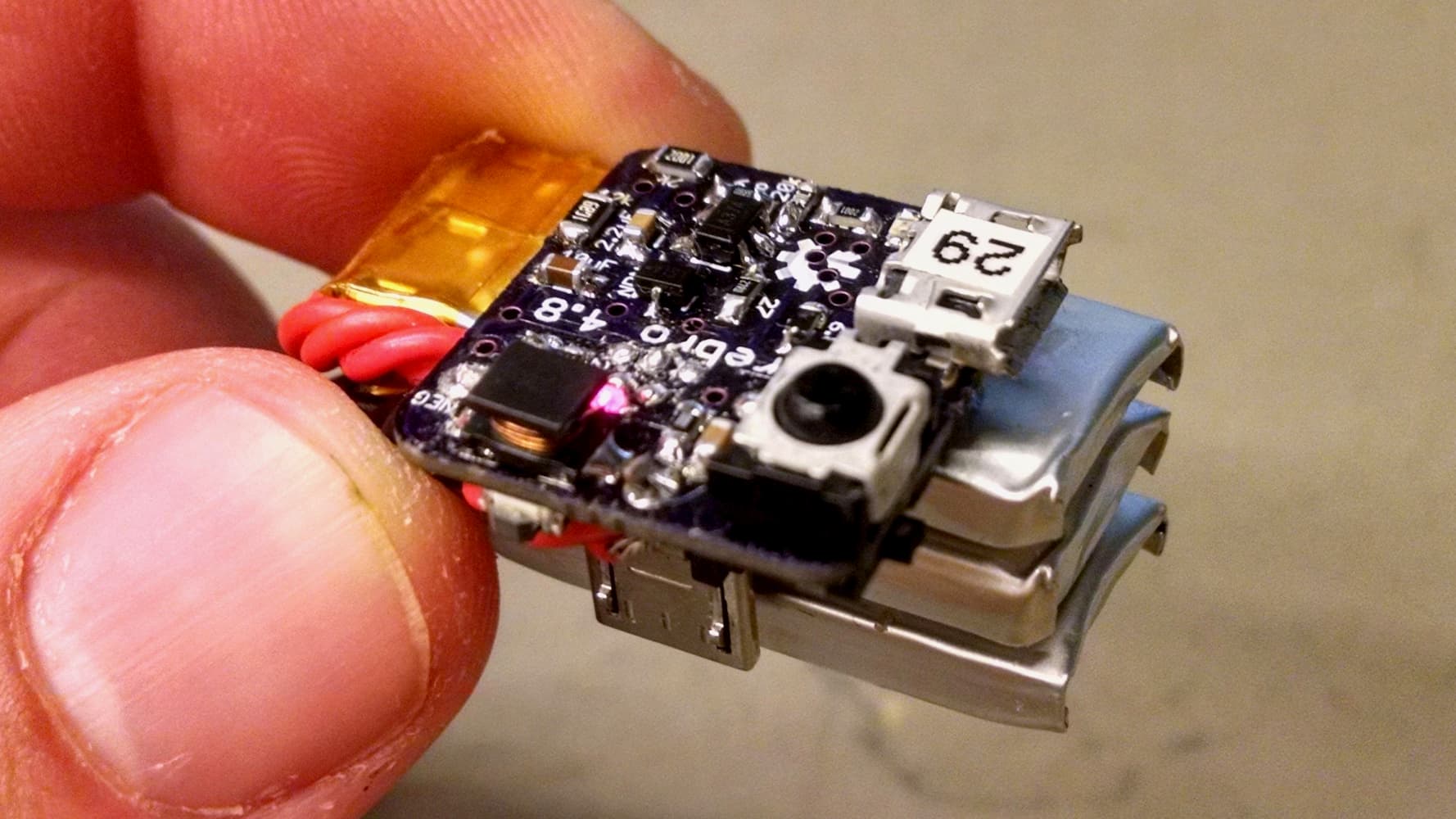
The behavior task used in my lab involves a rat rapidly moving left to right, hitting levers and poking its nose into holes. A common way to implement optogenetics is to shine light from a laser through a long optical fiber that is implanted in the brain. However this tethered configuration had a significant negative effect on the rat’s performance at our behavior task. Therefore it was my job to create an untethered solution. The receiver needed to be small/light enough to be placed on a rat’s head, have a short and determinant latency, and last for 4-5 hour sessions.
Wireless Communication
I chose to use an infrared (IR) LED paired with an IR sensor as a means of communication. This is the exact same technology used for TV remotes.
Its first advantage is its low power consumption. The IR sensor only passively receives signals and therefore doesn’t spend energy transmitting messages or trying to maintain a connection.
Its second advantage is it simplicity. Whereas something like Bluetooth Low Energy has a nearly 3000 page specification and entire books written on how to use it, IR communication is very straightforward. An IR sensor hangs out on your circuit outputting a high signal. If it is hit by a specific wavelength of light AND that light is being modulated at a specific frequency, it outputs a low signal. In my case I’m using a Base Station to turn a 940nm LED on and off at 38kHz.
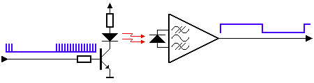
IR light (flickered at 38kHz) is received by the IR sensor which then outputs corresponding low signals. Source: SB-projects
Because of the simplicity, I have the flexibility to create my own communication protocol that fulfills my specific needs. The protocol I came up is optimized to minimize latency while at the same time preventing false positives.
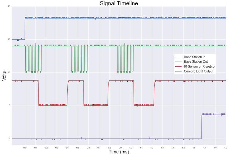
Signal Breakdown
Receiver Circuit design
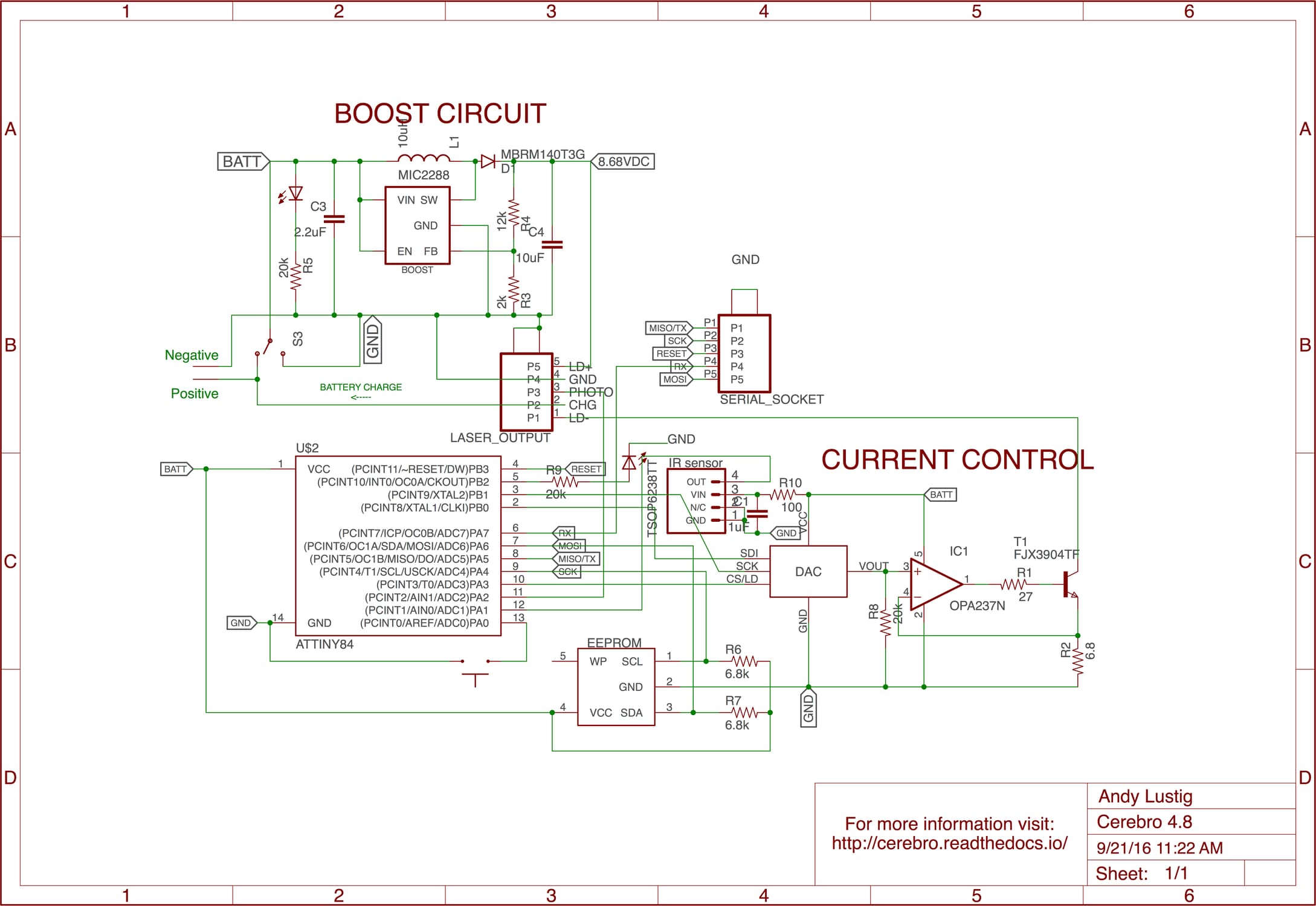
Wireless receiver schematic
Boost Converter
Most of the circuitry runs of off the lipo battery at 4.2 Volts. The laser diodes however need to be powered by upwards of 8.5 Volts, so there is a boost converter that…ya know…boosts the voltage that is provided to the laser diodes.
Laser output
This male micro USB plug connects to either a head implant PCB to provide laser diodes power, or it plugs into a charging dock to provide an easy means for recharging on-board lithium polymer (lipo) batteries.
Serial Socket
This serves as a ISP port for the MCU. It also serves as a serial output for downloading log data from the EEPROM via the downloader cord.
8-bit Microcontroller (MCU)
The brains behind everything. It deciphers commands received by the IR sensor, controls the DAC, and talks to the EEPROM
EEPROM
Non-volatile memory that the MCU can read and write information from/to. Every command that is wirelessly received is immediately logged to memory (along with a timestamp). This reception log can then be downloaded from Cerebro to the computer and cross-checked with a separate transmission log to make sure every message that was sent was in fact received.
DAC, op-amp, and transistor (Current Control)
So this is my favorite part of the circuit. We can control the current going to the laser diodes with a resolution of 90 μA using three major components: a digital to analog converter (DAC), an op-amp, and a transistor.
The laser diodes are on the high side of the transistor with a boosted voltage trying to push current through. The only path for the current to flow to ground is through the transistor, which acts like an adjustable valve for the current. When the transistor is off so are the laser diodes. When the transistor is on, and therefore letting current flow, the laser diodes emit light.
The MCU first talks to the DAC telling it to output a voltage from 0 - 2.5 Volts. The output voltage goes into an op-amp that then outputs a voltage at R1. Changing this voltage at R1 changes the current going into the base of a transistor. Adjusting the current at the base of the transistor is how the “valve” is adjusted, allowing more or less current flow from its collector to its emitter. The current leaves the transistor’s emitter and goes through R2 to ground.
This is where it gets pretty cool…we connect the voltage across R2 as negative feedback into the op-amp. The op-amp will do everything in its power to keep the voltage difference between its inputs at 0. In other words, the op-amp will adjust its output until the voltage being fed back into its negative input is equal the voltage provided at its positive input.
Everything will hopefully make more sense if we work backwards. Say we want to provide the laser diodes with 200 mA. The same 200 mA that would go through the laser diodes, would also go through the transistor and then through R2. Using ohm’s law (Voltage = Current x Resistance) we can determine that 200 mA would create a voltage across R2 of 1.36 volts. Therefore we know we want 1.36 volts at R2 because that indicates that 200 mA of current is flowing through the laser diodes.
Okay, how do we get 1.36 volts at R2? Remember that the op-amp will do everything in its power to match the voltages at its inputs. So we simply give the op-amp 1.36 volts at its positive input. It will adjust its output, which in turn adjusts the current flowing through the transistor, until it receives 1.36 volts being fed back into its negative input.
How do we give 1.36 volts to the op-amps positive input? We’re using a digital to analog converter (DAC) that has 12-bits of resolution. We use the MCU to send a digital value from 0-4095, and the DAC will output a corresponding voltage from 0-2.5 volts. So if we want 1.36 volts we need to send the DAC a value of 2228 because 1.36 / 2.5 x 4095 = 2228.
So there you have it, to get 200 mA flowing through the laser diodes we send a value of 2228 to the DAC.
Software and Documentation
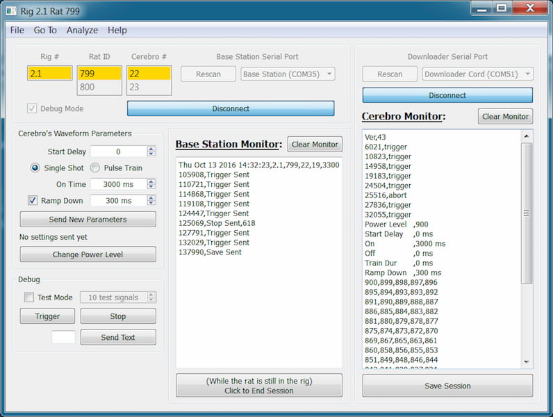
Building a GUI
I used Qt, a C++ framework for making applications, to make a Windows GUI.
Documentation
I wrote extensive documentation (check it out here!) for building and using the system. The docs are written in reStructuredText markup language, generated into HTML by Sphinx, and hosted on the web using Read The Docs.
System Components
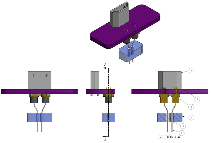
Head implant CAD
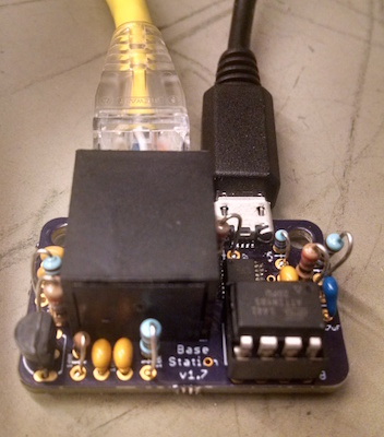
The Base Station is mounted to the top of the behavior rig and sends wireless commands to Cerebro using an infrared LED
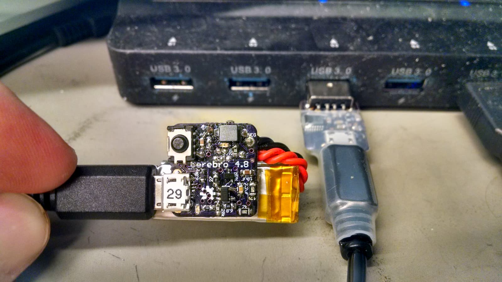
Cerebro connected to Downloader Cord
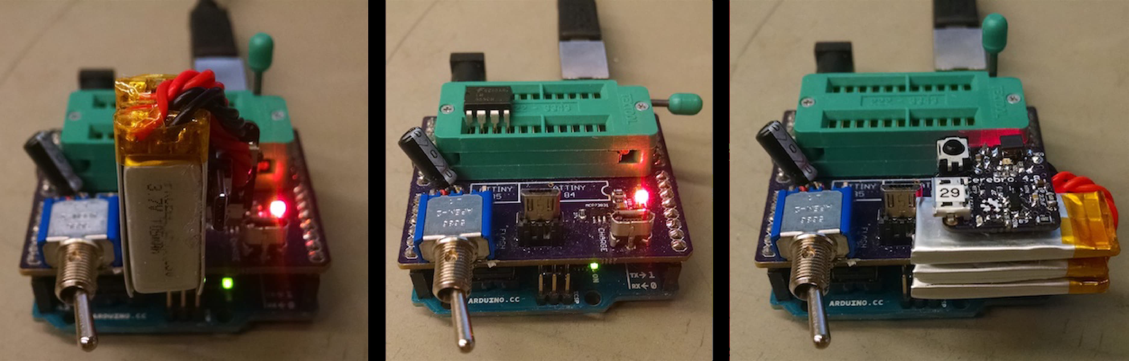
Utility shield has connections for programming Cerebro, programming Base Station, and charging Cerebro
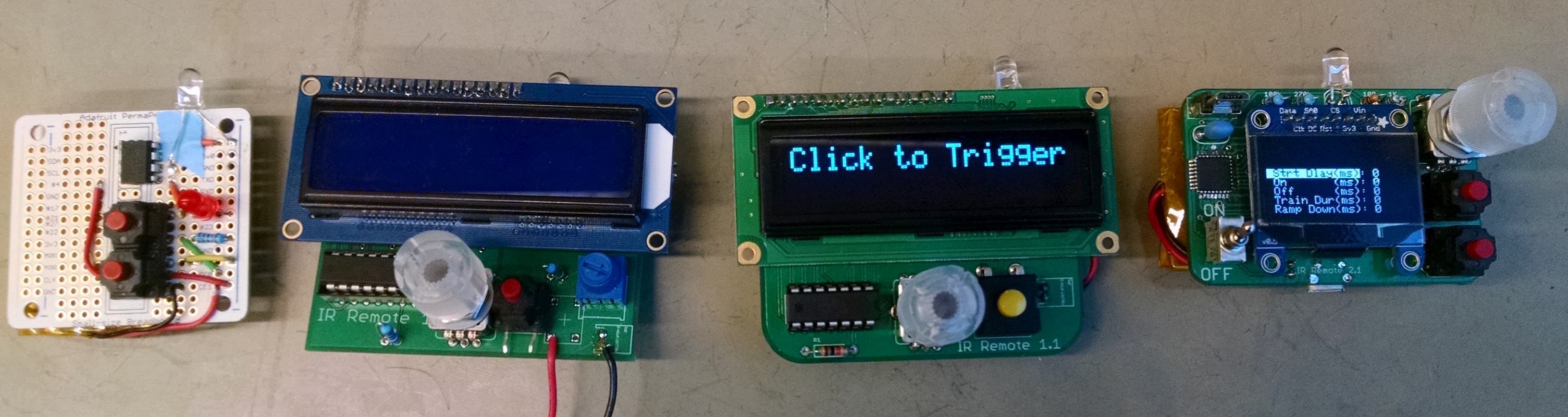
Evolution of IR Remote